Mainboard Information
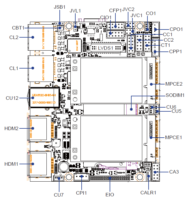
Mainboard Layout View
The following layout shows the connectors location on the mainboard.
List of Jumpers
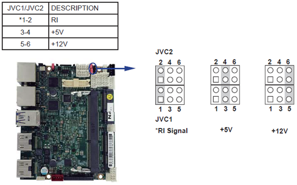
JSB1: CMOS DATA clear JVL1: LCD Panel power select JVC1/JVC2: COM1/2 RI & power select
Jumper Setting Description
A jumper is ON as a closed circuit with a plastic cap covering two pins. A jumper is OFF as an open circuit without the plastic cap. Some jumpers have three pins, labelled 1, 2, and 3. You could connect either pin 1 and 2 or 2 and 3. The below figure shows the examples of different jumper settings in this manual.
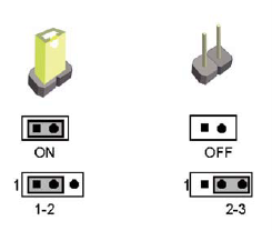
All jumpers already have its default setting with the plastic cap inserted as ON, or without the plastic cap as OFF. The default setting may be referred in this manual with a ” * ” symbol.
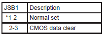
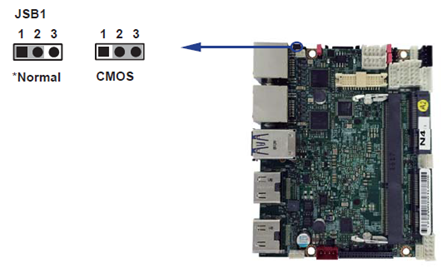
JSB1: CMOS Data Clear
A battery must be used to retain the motherboard configuration in CMOS RAM. Close Pin1 and pin 2 of JSB1 to store the CMOS data. To clear the CMOS, follow the procedures below:
Turn off the system and disconnect the power
Remove DC 12V power cable from DC 12V power connector
Locate JSB1 and close pin 1-2 for few seconds
Return to default setting by close pin 1-2
Connect DC 12V power cable back to DC 12V Power connector
Do not clear CMOS unless you are a) troubleshooting or b) forgot the BIOS Password
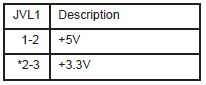
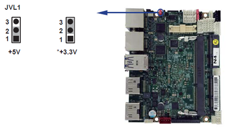
JVL1: LCD panel power select
JVC1/JVC2: COM1/2 Ring Indicator and power select